

Author: Andrea Biagioni, INFN
One of the goals of RED-SEA is to tightly integrate network interfaces to different computing nodes, accelerators and workloads. We are addressing interfaces with ARM and RISC-V to prepare a number of EPI-related IPs for the new interconnect, but more generally we are designing an effective network interface for different workloads to create a highly heterogeneous programmable platform that can be connected to state-of-the-art interconnect technologies.
In other words we propose different network interface cards for different workload scenarios. Each network interface card is one end-point of the BXI environment, having specialized Network interface for the target application and offering a BXI link as the I/O interface.
Within RED-SEA, INFN designs and implements the network interface card APEnetX based on a PCIe interface to communicate with CPU and GPU accelerators, and prototyped it exploiting Xilinx Alveo FPGAs.
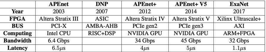
The Array Processor Experiment (APE) is an INFN initiative aiming to design an innovative HPC computing platform partnered by several physics’ institutions all over the world; since its start in 1984, it has developed four generations of MPP custom machines (APE [1], ape100 [2], APEmille [3] and apeNEXT [4]). Leveraging the acquired know-how in networking and re-employing the gained insights, a spin-off project called APEnet developed an interconnect board based on FPGA to build a 3D torus direct network architecture for PC Cluster.
The design of APEnet interconnect is portable and has been deployed in different environments: (i) the APEnet [5] was the first point-to-point, low-latency, high-throughput network interface card for LQCD dedicated clusters; (ii) the Distributed Network Processor [6] (DNP) was one of the key elements of RDT (Risc+DSP+DNP) chip for the implementation of a tiled architecture in the framework of the EU FP6 SHAPES project [7]; (iii) the APEnet+ Network Interface Card, based on an Altera Stratix IV FPGA, was developed in the framework of the EU FP7 EURETILE project and deployed in a hybrid, GPU-accelerated x86 cluster QUonG [8] implementing a 3D toroidal mesh topology able to scale up to 104 ÷ 105 nodes. APEnet+ was the first device integrating GPUDirect RDMA capabilities allowing for direct access to the memory of the NVIDIA GPU and lowering GPU-to-GPU latency; (iv) the APEnet network IP — i.e. routing logic and link controller — is responsible for data transmission at Tier 0/1/2 in the framework of H2020 ExaNeSt [9] project. Finally, EuroEXA leverages on ExaNet to push the concept of “hybrid topology scalable interconnect” (Trifecta™) at extreme scale. INFN designed an innovative “Custom Switch” based on a single FPGA Virtex Ultrascale+ implementing 2-hops all-to-all topology at board level, a 3D Torus network at rack level and a ExaNet-Ethernet 100/200G bridge for inter-racks connectivity.
APEnet Interconnect architecture
The APEnet interconnect has at its core the the Distributed Network Processor (DNP) acting as an offloading network engine for the computing node, performing internode data transfers; the DNP has been developed as a parametric Intellectual Property library; there is a degree of freedom in choosing some fundamental architectural features, while others can be customized at design-time and new ones can be easily added. The APEnet architecture is based on a layer model, as shown in Figure 2, including physical, datalink, network, and transport layers of the OSI model.
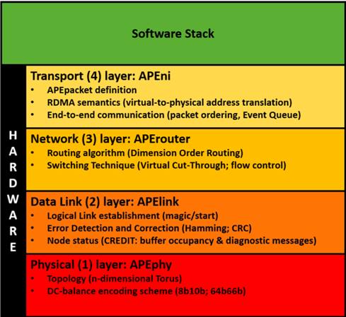
The physical layer — APEphy — defines the data encoding scheme for the serial- ization of the messages over the cable and shapes the network topology. APEphy provides point-to-point bidirectional, full-duplex communication channels of each node with its neighbours along the available directions (i.e. the connectors composing the IO interface). APEphy is strictly dependent on the embedded transceiver system provided by the available FPGA. It is normally based on a customization of tools provided by the FPGA vendor — i.e. DC-balance encoding scheme, deskewing, alignment mechanism, byte ordering, equalization, channel bonding. In APEnet+ and APEnet+ V5, four bidirectional lanes, bonded into a single channel with usual 8b10b encoding, DC-balancing at transmitter side and byte ordering mechanisms at receiver side, allow to achieve the target bandwidth (34 Gbps [10] and 45 Gbps [11] respectively).
The data-link layer — APElink — establishes the logical link between nodes and guarantees reliable communication, performing error detections and corrections. APElink [12] is the INFN proprietary high-throughput, low-latency data transmission protocol for direct network interconnect based on word-stuffing technique, meaning that the data transmission needs submission of a magic word every time a control frame is dispatched to distinguish it from data frames. The APElink manages the frame flow by encapsulating the packets into a light, low-level protocol. Further, it manages the flow of control messages for the upper layers describing the status of the node (i.e. health status and buffer occupancy) and transmitted through the APElink protocol.
The network layer — APErouter — defines the switching technique and routing algorithm. The Routing and Arbitration Logic manages dynamic links between blocks connected to the switch. The APErouter applies a dimension order routing [13] (DOR) policy: it consists in reducing to zero the offset between current and destination node coordinates along one dimension before considering the offset in the next dimension. The employed switching technique — i.e. when and how messages are transferred along the paths established by the routing algorithm, de facto managing the data flow — is Virtual Cut-Through [14] (VCT): the router starts forwarding the packet as soon as the algorithm has picked a direction and the buffer used to store the packet has enough space. The deadlock-avoidance of DOR routing is guaranteed by the implementation of two virtual channels [13] for each physical channel.
The transport layer — APE Network Interface — defines end-to-end protocols and the APEpacket. The APE Network Interface block has basically two main tasks: on the transmit data path, it gathers data coming in from the bus interfacing the programming sub-system, fragmenting the data stream into packets — APEpacket— which are forwarded to the relevant destination ports, depending on the requested operation; on the receive side, it implements PUT and GET semantics providing hardware support for the RDMA (Remote Direct Memory Access) protocol that allows to transfer data over the network without explicit support from the remote node’s CPU.
The full APE Network Interface offers a register-based space for configuration and status signaling towards the host. Further, it offers a variable size region for defining several ring buffers, each one linked to an OS process accessing the device. These regions are typically accessed in slave mode by the host, which is master (read/write of single 32-bit based registers). A certain number of DMA engines are used to move data to and from the device, plus other additional services: a TX descriptor queue (to issue buffer transfers from host to device) and an event queue (to notify different kind of completions to host). Single or Multiple DMA engines could manage the same intra-tile port.
APEnetX board
APEnetX, a low-latency and high-throughput NIC based on a PCIe Gen3/Gen4 interface, is the latest generation of APEnet interconnect architecture.
The APEnetX prototype is developed on a Xilinx Alveo U200 board, which is built on the Xilinx 16nm UltraScale architecture and natively supports the QDMA IP. PCIe support is developed using QDMA IP by Xilinx, on the leftmost part of the figure 3: in green the routing and switching IP and the transmission control logic developed mainly during past European projects and optimized to meet the requirements of the RED-SEA project; the proposed Network Interface (APEni) supporting the RDMA semantics is in blue which manages the user-level, zero-copy RDMA data transmission to/from memory and offloads the host operating system. In the current implementation the virtual memory address resolution is managed through the IOMMU of the Intel processor for the implementation of the direct I/O.
Xilinx provides an open-source device driver for the QDMA IP to be used as hardware validation and demonstrator. A user-space software stack to highlight the performances that the design can hit is also included. We modified the Xilinx software, adding custom features and trying to reuse as much as possible the available code avoiding the loss of compatibility with new versions that could be released in the future.
A first optimization is to have a different completion address for every receiving buffer. The user-space software checks only a single memory area, allocated in the memory address space of the user process and then remapped in the kernel memory address space, where the kernel copies the new completion.
Results
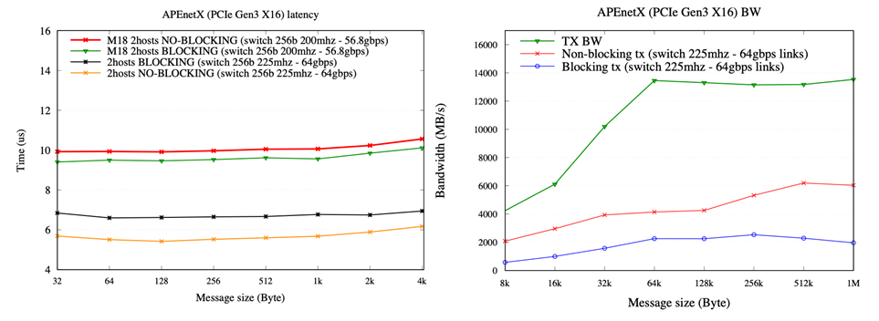
To validate the hardware design and the software stack, we used a testbed composed by two Supermicro SuperWorkstation 7049GP-TRT, 2 × 8-cores 4200-series 14nm Intel Xeon Scalable Silver Processors (Cascade Lake) running at 2.10GHz with PCIe GEN3 support and a total memory of 192GB DDR4 at 3.2GHz. As operating system, we used a GNU/Linux Centos 8 with a 4.18.0 kernel. Two different APEnetX boards are connected point-to-point through custom “apelink” protocol with QSFP+ cables. The preliminary results for latency and bandwidth are reported below.
References
[1] M. Albanese et al., “The ape computer: An array processor optimized for lattice gauge theory simulations,” Computer Physics Communications, vol. 45, no. 1, pp. 345 – 353, 1987.
[2] C. Battista et al. “The ape-100 computer: (i) the architecture,” International Journal of High Speed Computing, vol. 05, no. 04, pp. 637–656, 1993.
[3] F. Aglietti et al., “The teraflop supercomputer apemille: architecture, software and project status report,” Computer Physics Communications, vol. 110, no. 1, pp. 216 – 219, 1998.
[4] F. Belletti et al., “Computing for lqcd: apenext,” Computing in Science Engineering, vol. 8, no. 1, pp. 18–29, Jan 2006.
[5] R. Ammendola et al. “APENet: LQCD clusters a la APE,” Nuclear Physics B-Proceedings Supplements, vol. 140, pp. 826–828, 2005.
[6] A.Biagioni et al’, “The Distributed Network Processor: a novel off-chip and on-chip interconnection network architecture,” arXiv:1203.1536, Mar. 2012,
[7] R. Leupers et al., “Shapes:: a tiled scalable software hardware architecture platform for embedded systems,” in Proceedings of the 4th International Conference on Hardware/Software Codesign and System Synthesis (CODES+ISSS ’06), Oct 2006, pp. 167–172.
[8] R. Ammendola et al., “QUonG: A GPU-based HPC system dedicated to LQCD computing,” in Application Accelerators in High- Performance Computing (SAAHPC), 2011 Symposium on, July 2011, pp. 113–122.
[9] M. Katevenis et al., “Next generation of Exascale-class systems: ExaNeSt project and the status of its interconnect and storage development,” Microprocessors and Microsystems 61, 58 (2018)
[10] R. Ammendola et al., “A 34 Gbps data trans- mission system with FPGAs embedded transceivers and QSFP+ modules,” in Nuclear Science Symposium and Medical Imaging Conference (NSS/MIC), 2012 IEEE, 2012, pp. 872–876.
[11] R. Ammendola et al., “Architectural Improvements and Technological Enhancements for the APEnet+ Interconnect System,” Journal of Instrumentation, vol. 10, no. 02, p. C02005, 2015. [Online]. Available: http://stacks.iop.org/1748-0221/10/i=02/a=C02005
[12] R. Ammendola et al., “APEnet+ 34 Gbps Data Transmission System and Custom Transmission Logic,” Journal of Instrumentation, vol. 8, no. 12, p. C12022, 2013. [Online]. Available: http://stacks.iop.org/1748-0221/ 8/i=12/a=C12022
[13] W. J. Dally and C. L. Seitz, “Deadlock-free message routing in multiprocessor in- terconnection networks,” Computers, IEEE Transactions on, vol. C-36, no. 5, pp. 547–553, 1987.
[14] P. Kermani and L. Kleinrock, “Virtual Cut-Through: A New Computer Communication Switching Technique,” Computer Networks, vol. 3, pp. 267–286, 1979.